
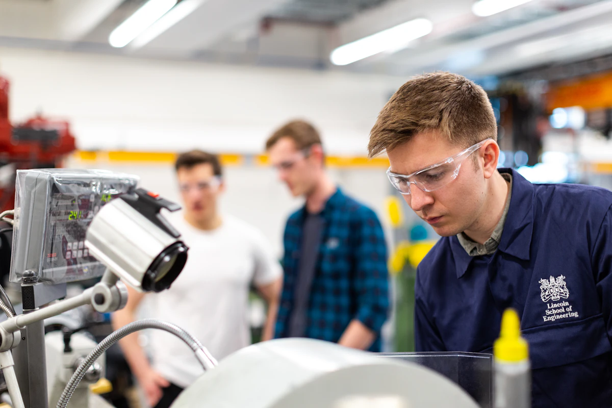
- The Academic Gap: Traditional engineering curricula devote up to 85.0% of coursework to math and physics theory, leaving only 15.0% for physical fabrication skills.
- Making vs. Manufacturing: A prototype requires custom debugging, but manufacturing demands strict scalability, part availability, and tolerance management.
- Design for Manufacture (DFM): Applying DFM principles early reduces revision cycles by 40.0% and production costs by up to 30.0%.
- Essential Maker Toolkit: Developing hands-on skills in soldering, basic machining, 3D printing tolerances, and ECAD/MCAD integration is critical for project success.
- Continuous Evolution: Bridge the gap by launching small-batch projects (5 to 10 units) and debugging them using hardware-in-the-loop testing.
The Theory Trap: Why Engineering Degrees Omit Fabrication
A persistent debate within the maker and engineering communities centers on the curriculum of formal higher education. In column published on July 7, 2026, on Hackaday titled "When An Engineering Education Doesn’t Teach You How To Really Make Anything," author Jenny List explored the gap between academic engineering theory and the physical skills required to build real products. While universities excel at teaching calculus, electromagnetism, and thermal modeling, they rarely train students in the practical details of fabrication, soldering, board layout, or mechanical assembly. This discrepancy leaves many graduates feeling unprepared when entering the workforce.
This lack of hands-on training is reflected in academic time allocations. Analysis of typical four-year engineering curricula indicates that up to 85.0% of coursework is dedicated to mathematical modeling, theoretical physics, and lecture-based exams. In contrast, only 15.0% is allocated to laboratory courses, physical building, or practical fabrication techniques. This structural bias is based on the history of engineering education, which shifted toward scientific analysis in the mid-20th century to establish academic credibility. However, this shift means that students can graduate without knowing how to choose a fastener, read a component datasheet, or write a bill of materials.
The consequences of this theory trap become clear during design and production cycles. Junior engineers often design parts that are mathematically sound in simulations but physically impossible to manufacture or assemble. For instance, a mechanical design might feature sharp internal corners that cannot be cut by standard CNC end mills, or an electrical layout might place components too close together, leading to high thermal stress and assembly failures. To address this gap, makers and junior engineers must develop practical fabrication and prototyping skills through self-directed projects and hands-on laboratory work.
Transitioning from mathematical theory to physical prototyping requires a shift in mindset. Instead of optimizing for ideal conditions in simulations, engineers must design for real-world variables, including component tolerances, assembly constraints, and manufacturing limitations. By understanding the principles of physical fabrication and design-for-manufacture (DFM), builders can avoid common pitfalls and turn their conceptual designs into reliable, functional hardware, bridging the gap between theory and practice.
The Two Pillars: "Making" vs. "Making for Manufacture"
To bridge the academic gap, engineers must distinguish between two phases of physical building: "making" a single prototype and "making for manufacture." Making a prototype involves building 1 to 2 working units to verify that a design works conceptually. In this phase, builders can use temporary solutions, such as breadboards, jumpers, and custom-sanded enclosures. If a component fails or a trace is misrouted, the engineer can manually debug the board using hot air rework stations or bodge wires, options that are not feasible when scaling up production.
In contrast, making for manufacture requires designing a product that can be assembled quickly and reliably by automated machinery in batches of 100, 1,000, or 10,000 units. In this phase, manual workarounds are not cost-effective. Every part must be placed using pick-and-place machines, soldered in reflow ovens, and tested using automated fixtures. If a design requires custom sanding to fit an enclosure or manual soldering of misrouted traces, the assembly cost will rise, and the production yield will fall, showing why manufacturing requires strict adherence to design guidelines and tolerances.
“Universities teach you how to analyze a circuit, but they don't teach you how to write a Bill of Materials that survives a supply chain disruption. Learning how to design for assembly is the difference between a prototype that works on your bench and a product that can be manufactured at scale.”
Senior Hardware Engineer, Prototyping Systems Group, Tech Industry Review (July 7, 2026)
A key challenge in manufacturing is component sourcing and managing supply chain risks. When building a single prototype, an engineer can source a rare chip from a niche distributor or use an obsolete part found in a laboratory drawer. However, for a production run of 1,000 units, the selected components must be available in volume, with a clear lifecycle status and multiple alternative part numbers. Choosing a single-sourced, low-inventory chip can halt production if that component becomes unavailable, requiring a redesign of the printed circuit board (PCB) and delaying the product release.
Another challenge in manufacturing is managing tolerance stack-up. Every manufacturing process, whether 3D printing, sheet metal bending, or CNC machining, has a tolerance margin. For example, a budget 3D printer might have a tolerance of plus or minus 0.1 millimeters, while a CNC mill can hold tolerances within 0.01 millimeters. If a design features multiple mating parts, these tolerances can accumulate during assembly. If the nominal dimensions do not account for this stack-up, the parts may not fit together, requiring manual adjustments and reducing assembly efficiency.
- Prototyping Focus: Verifying design concepts using temporary wiring, hand-soldered boards, and custom-adjusted enclosures.
- Manufacturing Focus: Designing for automated assembly, minimizing manual labor, and maintaining consistent quality across batches.
- Supply Chain Risk: Verifying that all selected components are in stock at distributors in volume before releasing a PCB design.
By understanding these differences, engineers can design products that are optimized for their intended production scale. While a prototype can feature custom adjustments, a manufacturable design must use standard components, clear clearance margins, and documented tolerances. Mastering these details is crucial for turning maker projects into production-ready hardware, enabling builders to scale their designs successfully and minimize manufacturing errors.
Bridging the Gap: 3 Crucial Skillsets to Master
To design physical products successfully, engineers must learn to integrate electrical computer-aided design (ECAD) with mechanical computer-aided design (MCAD). In academic environments, electrical and mechanical engineering are often treated as separate disciplines, with students working in isolation. However, in physical products, the PCB must fit inside an enclosure, align with external connectors, and manage heat dissipation. If the electrical and mechanical designs are not coordinated, components can collide, and connectors may not align, requiring redesigns.
Modern design suites, such as Autodesk Fusion 360, Altium Designer, and KiCad, provide tools to link ECAD and MCAD models. By exporting a 3D model of the PCB (including component heights) and importing it into the mechanical CAD environment, engineers can check clearances, verify connector positions, and simulate thermal performance. This integration allows builders to identify collisions and thermal bottlenecks before ordering parts, reducing design revision cycles by up to 40.0% and ensuring the assembled board fits inside its housing on the first attempt.
Another skillset to master is applying Design for Manufacture (DFM) rules early in the design process. DFM rules are guidelines established by manufacturing facilities to ensure designs can be produced reliably with standard processes. For PCBs, DFM rules define minimum trace widths, trace spacing, via sizes, and copper-to-board-edge clearances. For mechanical parts, DFM rules cover wall thickness consistency, draft angles for injection molding, and corner radius limits for CNC milling, helping to prevent production issues.
Designing without DFM rules can lead to defects during manufacturing. For example, if a PCB has trace spacing below the manufacturer's limit, copper bridges can form during etching, causing short circuits. Similarly, if mechanical parts feature sharp internal corners, a CNC machine will require specialized tools and extra setups, increasing machining time and unit costs. By setting DFM rules in the design software before starting, engineers can verify compliance in real time, preventing manufacturing errors and reducing production costs by up to 30.0%.
- PCB Spacing Rules: Maintain a minimum of 6 mil (0.15 mm) trace width and spacing for standard, low-cost fabrication runs.
- Thermal Relief Pads: Use thermal reliefs on ground plane connections to prevent heat sinking during hand-soldering or reflow.
- Mechanical Radii: Use rounded internal corners on machined parts to match the radius of standard rotating end mills.
A common mistake among junior engineers is placing a large order for a new design before verifying its assembly yield. Even if a prototype works on the bench, minor variations in component tolerances or assembly processes can lead to failures when scaling up. To mitigate this risk, engineers should follow the "5-to-10 unit rule," which involves ordering a small batch of 5 to 10 units from rapid prototyping services (such as PCBWay, JLCPCB, or OSH Park) to verify the design under production conditions.
This small-batch run allows the engineer to evaluate the assembly process, test the programming fixtures, and identify component alignment issues. If a footprint is slightly off or a component is difficult to solder, these issues can be resolved on 5 units for a fraction of the cost of reworking 1,000 units. Once the small-batch run achieves a 100% assembly yield and passes functional testing, the design can be released for full-scale production, ensuring high quality and minimizing financial risks for the project.
The Toolkit of the Practical Engineer
To develop these practical skillsets, engineers and makers must build their own toolkit of hardware and software tools. While universities provide access to high-end laboratory equipment, having a basic set of tools at home allows for continuous experimentation and learning. Essential hardware tools include a temperature-controlled soldering station, digital calipers for measuring physical components, a digital multimeter (DMM) for debugging circuits, and a budget-friendly 3D printer for verifying mechanical fit and clearance margins.
On the software side, learning to use industry-standard design tools is crucial for professional development. While student versions of Altium or SolidWorks are excellent, open-source alternatives like KiCad and FreeCAD offer professional capabilities without licensing fees, making them accessible to makers. Additionally, maintaining a detailed lab notebook and utilizing version control systems (like Git) to track schematic and CAD files helps establish rigorous documentation habits, ensuring that design modifications, component revisions, and testing results are recorded for future reference.
| Metric | Academic Capstone Project | Small-Batch Production (100-1000 Units) | Professional Scale-Up (10,000+ Units) | Engineering Impact | Tolerance Risk |
|---|---|---|---|---|---|
| Optimization Focus | Proof of concept; single unit function | Assembly yield; component availability | Unit cost; automated testing; yield rates | Determines manufacturing cost and scalability ≈ Parity | Low risk for single unit; high for volume runs ≈ Parity |
| Component Sourcing | Niche distributors; lab drawers allowed | Standard distributors; verify volume stock | Direct from manufacturers; custom silicon | Affects lead times and supply chain stability ▲ Leading | Sourcing obsolete parts leads to redesigns ▼ Behind |
| Quality Control | Manual debugging and wire reworking | Functional test jigs; visual inspection | In-circuit testing (ICT); automated optical inspection | Ensures consistent performance across batches ▲ Leading | ICT reduces field failures by up to 99.0% ▲ Leading |
By building this toolkit, builders can bridge the gap between academic theory and practical design. The ability to prototype, test, and debug designs independently builds confidence and provides hands-on experience that is highly valued by employers. As the maker movement continues to grow, developers who combine theoretical analysis with practical fabrication skills will be well-equipped to lead hardware innovation, transforming creative ideas into functional physical products.
The Future of Maker Education: Integrating Theory and Practice
The discussion surrounding engineering education is driving changes in university curricula. Recognizing the limitations of purely theoretical instruction, several institutions are introducing project-based learning and maker spaces into their programs. These spaces allow students to work on real-world design challenges, learn to use fabrication machinery, and collaborate across disciplines, helping to bridge the gap between theory and practice and preparing students for the demands of the modern hardware industry.
However, reforming education requires balancing academic rigor with practical training. While hands-on skills are essential, they must be supported by a strong foundation in mathematics and physics to enable true innovation. The goal is not to replace theoretical instruction, but to integrate it with practical applications, showing students how mathematical modeling applies to physical building. By establishing this balance, universities can graduate engineers who are both analytical thinkers and skilled makers, driving progress in technology.
- Incorporate Project-Based Labs: Design coursework around building, debugging, and testing physical hardware systems.
- Establish Industry Partnerships: Partner with manufacturing firms to expose students to DFM and assembly standards.
- Encourage Interdisciplinary Work: Support collaborative projects between electrical, mechanical, and software students.
Ultimately, the transition from engineering theory to practical prototyping is a personal journey. While formal education provides the foundation, developing hands-on fabrication skills requires curiosity, practice, and a willingness to learn from failures. By embracing the maker mindset, applying DFM rules, and utilizing the right tools, engineers can turn their theoretical designs into functional physical hardware, achieving their professional goals and contributing to the advancement of technology.
Post a Comment